December 3, 2017 – Using light instead of electrons is the future of computing. Photons that transmit data at the speed of light can pack even more data crunching into our digital machines and allow us to make the processors in them even smaller. Today we are reaching the limits of Moore’s Law. It is getting harder to shrink components when we process information using electrons because that requires wires even if they are nano-sized. But with photons instead of wire, we will use glass in our computers as the data transmission medium in the same way telecommunications and Internet service providers use fiber optic cables. Those cables deliver the Internet to our front door at blindingly fast speeds. But once it gets to us our wire-based modems, computing technology, tablets, and smartphones convert photon-streamed data into electrons delivered by wires or WiFi.
But it appears that we may soon see photonic computing based on work being done at the Imperial College London, in the United Kingdom, where light is being used to transmit large volumes of data while emitting little to no heat. How is this possible? The researchers are using metamaterials to squeeze photons into channels a mere 25 nanometers wide transmitted over distances measured in micrometers rather than centimeters. That means light circuits capable of replacing transistors, the devices that are crammed onto today’s computer chips. And that also means even smaller chips that are faster.
The researchers have also addressed another challenge brought on by using light rather than electrons in data transmission within a digital device. Normally when electrons cross each other in a computing device they interact. Photons when they cross each other don’t. So keeping them separate requires what these researchers have developed, a plasmonic nanofocusing waveguide to confine the light beams to individual channels within the medium used to construct the light circuits.
The research has been published in the December 1, 2017, edition of the journal Science, in an article entitled “Giant nonlinear response at a plasmonic nanofocus drives efficient four-wave mixing.”
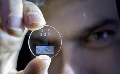
Using glass for the next generation of computing devices is already beginning. New memory technology already uses glass as a data storage medium. At the University of Southampton, also in the United Kingdom, nanostructured glass is being used to create “eternal data archiving.” The nanostructures change how light travels through glass to create memory equivalent to what is seen in Superman movies, (see image below) the glass memory crystals storing the entire history, science, and technology from the planet Krypton.

Enter reality and we see five-dimensional (5D) memory storage in the form of optical discs so small you can hold them between your thumb and index finger. with each storing up to 360 Terabytes of data, and capable of withstanding temperatures as high as 1,000 Celsius (1,832 Fahrenheit) degrees, and lifetime data stability lasting 13.8 billion years.
So how far are we away from seeing computers using photons to process and store information? We’ve already got the latter figured out and all that’s left is to create commercial versions of the technology. The former, however, remains a few years away. We’ll probably see photonic data transmission chip technology in high-end computing platforms first and my best guess is sometime before 2020. A few years later the rest of us will be buying computers and other digital devices incorporating the technology, sometime between 2022 and 2025 I would think.
Related articles across the web

Related Posts
 Conversations About AI: Disrupting and Democratizing Education
 Will Americans Stage a “Managed Retreat” from Their Coastlines?
 New NASA Report Shows Sea Level Rise Is Accelerating: Causes and Consequences
 Robots in the News: From Tesla Optimus to BMW Figure and More
 Why Am I Left-Handed? Blame Tubulin Proteins for This Asymmetric Brain Twist
 Navigating the Future: AI and the Power Grid
 Investing In Space Ventures Is Hot Right Now
 Weaponized Mosquitoes Are Being Deployed to Reduce Vector-Borne Diseases


