
March 12, 2018 – Materials science is a field of both engineering and science that seeks new material discoveries and new ways to use existing materials. In his latest e-mail blast Peter Diamandis, of XPrize fame, describes how the field is converging with other areas in science and engineering in unexpected and exciting ways. Tools like the Materials Genome Project apply machine learning to the subject, and new engineering fabrication techniques allow for precision material builds, atom by atom, creating out of old materials a whole new generation of new applications. In this posting I have taken Diamandis’ words and added a few of my own to describe the driving forces within material science today and tomorrow. Enjoy the read.
Over 70 years ago, John Bardeen, Walter Brattain, and William Shockley sparked the semiconductor revolution with the fabrication of the first transistor. This fundamental technology now powers every aspect of science, innovation, and society. Projections put a $500 billion revenue tag on the semiconductor industry in 2018.
Nearly all products today rely on semiconductor materials science and its mightiest outcome, the transistor, which plays a decisive part in global computation, artificial intelligence (AI), and big data. The Economist magazine predicts that AI-related products and innovations will add nearly $16 trillion to GDP by 2030.
“Data to this century is what electricity was in….previous generations,” states Omkaram Nalamasu, Senior Vice President and Chief Technology Officer at Applied Materials. “Today, [we generate] something like 230 million tweets per day, 300 billion emails are sent per day, and about a hundred terabytes of data are loaded on Facebook every day. This pales in comparison to what is going to happen in the next five years. The data rate growth is about 80 percent.”
Worldwide data storage capacity is estimated to be around 6 zettabytes by 2020, each byte powered by semiconductor materials science. Exponential network and computation technologies including AI, the Internet of Things (IoT), the blockchain, autonomous vehicles, and the Internet itself are expected to generate orders of magnitude more data over the next five years than our current global storage capacity. The IoT network alone, projected to consist of over 50 million devices in 2020, will generate 600 zettabytes of information. That’s 100 times our current storage capacity of 6 zettabytes.
Once collected, how will we process and make sense of this data? The answer: advances in computational materials. It is materials breakthroughs, both in today’s semiconductor technologies and tomorrow’s quantum computers, that will be necessary to meet growing data storage and computation needs. That means breakthrough materials to manage it all. The exponential nature of Moore’s law, therefore, is converging with breakthroughs in materials discovery and production.
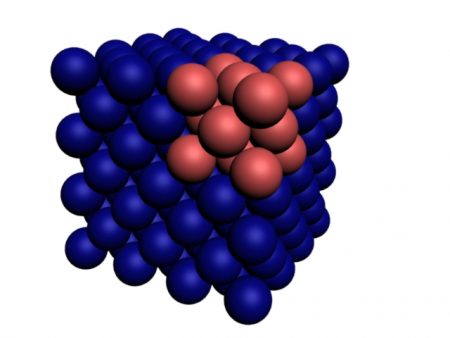
Machine Learning & Materials Discovery
Traditional materials science involves costly, in-lab iteration and theory-based guesswork. But by harnessing the power of supercomputers, quantum mechanics, and importantly, machine learning, materials engineers will be able to do in hours what used to take weeks, months or years.
To contextualize this acceleration, let’s look at Thomas Edison’s invention of the light bulb. Edison required a bulb with low heat production, low power consumption, and a long-lasting, light-emitting material. With intuition and empirical data as his guide, Edison set out testing over 1,600 materials. After 14 months of testing and tinkering, he settled on a carbon-coated cotton thread. Fast forward 30 years to the introduction of the tungsten filament and the market for Edison’s carbonaceous-cotton filament is wiped out. So Edison’s 1,600 experiments and guesses produced what ultimately was a sub-optimal material solution that readily was replaced within three decades.
But today materials engineers can work with materials discovery software to analytically derive and virtually test optimal new materials for specified applications. “Materials engineering is the ability to detect a very small particle — something like a 10-nanometer particle on a 300-millimeter wafer,” explains Nalamasu. “That is really equivalent to finding an ant in the city of Seattle.”
Thanks to machine learning and exponential leaps in computation and quantum theory, the high price of guesswork involved in materials discovery is rapidly being phased out in favor of analytical and numerical methods. The materials scientist of tomorrow will be able to specify desired properties of materials and with basic processing parameters, and a quantum-computer based machine learning program, return the optimal material composition required for a specific application. And materials innovation will lead to exponentially more materials innovations. Remember: supercomputers (and soon quantum computers) are the lineage of the computational materials disruption that has been taking place over the past 70 years.
Augmented Reality/Virtual Reality and Materials Science
Think back to the state-of-the-art mobile phone in the 1980s, big, bulky, and reserved for Wall Street executives. Phones ran upwards of $4,000 and weighed over 5 kilos (a dozen pounds). These phones could only be used for calls and lacked any memory to store contact information. “If you were to build a smartphone in 1980,” Nalamasu explains, “that would cost something like $110 million. It would be about 14 meters [about 45 feet] tall, and it would require about 200 kilowatts of energy… that’s the power of materials engineering.”
Today, thanks to materials science breakthroughs in semiconductor technology, touchscreen displays, and batteries, children and executives alike can access smartphones with a 6+ inch Organic Light Emitting Diode (OLED) touchscreen displays, 256+ gigabytes of storage, integrated 1080 pixel cameras, and endless other features. By the end of 2018, we’ll have over 2.5 billion smartphones like what I have described above in use according to projections.

Now let’s extrapolate the user interface moment for mobile devices allowed by materials science breakthroughs to the current state of augmented reality (AR) and virtual reality (VR).
Today, bulky, expensive, and hard-to-use VR headsets dominate the industry. These headsets are ripe for precisely the same types of materials breakthroughs that enabled the rise of the smartphone from its ancestor the bulky mobile phone.
Some of the materials breakthroughs anticipated to come in and accelerate VR technology:
- OLED display advances that allow headset resolution to increase from 500 pixels per inch to 3,000+ pixels per inch
- Optics to move from today’s traditional structures to thin films on the order of nanometers in thickness
- Memory improvements to store large VR graphics files
- Energy efficient processors and graphics cards to enable better, faster performance
- Battery advances to power the large energy requirements of running high-quality graphics
The future of AR and VR lies in sleek, slim, lightweight, and beautiful headsets that seamlessly integrate with our day-to-day lives. Thanks to coming materials advances, our future devices will be cheaper, thinner, faster and more powerful.